Wave Solder Pallets
Product Information:
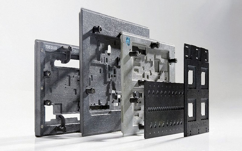
Wave soldering and SMT pallets are an essential and cost effective tool for the PCB assembly process. Pallet design allow for increased through put, the securing/aligning of critical components and allow for soldering of thru-hole components affected by bottom side SMT component layout violations.
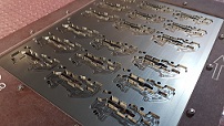
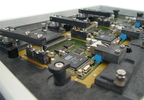
Wave soldering pallets are used for masking components of the bottom side of the PCB which are not to be soldered. Components to be soldered pass through the wave and get soldered. The pallet carries the entire board through the complete cycle.
Materials
Materials have now been designed for the wave solder and reflow PCB assembly process. Durapol, Durostone and Haysite have been adopted and are now the materials of choice. For the lead free wave solder and reflow process Durapol and Durostone have new formulation to withstand the higher temperature requirement and the more aggressive fluxes. All these materials are similar in their machining and durability characteristics.
Ordering Information
All we need is your PCB gerber file marked with any selective solder masking required on the underside. We will send 3D checkplot in 24hrs for checking. Produce prototype in 5 working days balance in 7 working days after checkplot confirmation.
| Pallet Complexity | Low | Medium | High |
|---|---|---|---|
| Thickness | up to 6mm | up to 8mm | up to 12mm |
| Pallet dimensions | up to 300mmx350mm | up to 300mmx400mm | up to 400mmx600mm |
| Qty of solder openings | up to 4 | up to 16 | up to 40 |
| Qty of step downs (except pcb pocket) | no stepdown | up to 4 | up to 10 |
Selective Soldering Pallets, Reflow Pallets, Adjustable Pallets and Component Holddown Pallets are produced from Durostone material, which is flux resistant and can operate till 380 degrees. 3D design is also prepared by experienced personnel for optimum results. We can offer several type of material.


Reflow Pallets
We recommend to use Reflow Pallets of Durostone Material, for your different PCB shapes, thin PCB material use to avoid warpages on your assembled board. You will be able to work effective with every kind of shapes and material thicknesses.
The following are the general data files required for fixture development. Products are processed differently. Supplying us with all of this data will ensure that we have what is needed for your application.
Top & Bottom Side Silkscreen
Top & Bottom Side Paste
Top & Bottom Side Mask
Fabrication Drawing
Drill Fab Layer
Other Requirements:
Height of components on the solder side of the PCB
Height of components requiring hold downs
Identify any components which overhang the board and whether they seat flush to the top of the PCB or receed to a certain depth


Selective Soldering pallets
Enables wave soldering of PTH components to Double Sided, mixed technology assemblies.
Selective soldering pallets allow the soldering of plated through hole (PTH) components to dual sided mixed technology assemblies while protecting solder side surface mount devices (SMD). The solder apertures are the areas that will expose your PTH leads to solder. These apertures have a sealing wall, much like a gasket, that presses against the circuit board to control the area that is exposed to the solder. Machined into the fixture are a series of pockets cut into the bottom surface that are engineered to promote solder flow to all the PTH areas.
Required general data files:
Top & Bottom Side Silkscreen
Top & Bottom Side Paste
Top & Bottom Side Mask
Fabrication Drawing
Drill Fab Layer
Other Requirements:
Height of components on the solder side of the PCB
Height of components requiring hold downs
Identify any components which overhang the board and whether they seat flush to the top of the PCB or receed to a certain depth


